
Nell'era digitale, i display a LED sono fondamentali in diverse applicazioni. Questo articolo si concentra su macchina distributrice a getto d'inchiostro: esplora come risolve le sfide dello sviluppo di display, crea strati uniformi di emissione luminosa, interagisce con le apparecchiature SMT e influisce sui contrasti di packaging COB/SMD. Consiglia inoltre i migliori strumenti per la stampa a getto d'inchiostro, evidenziandone il ruolo nell'innovazione dei display a LED.
Sommario
AlternaNozioni di base sul funzionamento del display a LED
Principio di luminescenza del chip LED
Il LED, abbreviazione di diodo a emissione luminosa, è costituito da un chip semiconduttore, comunemente costituito da composti di gallio (Ga) con arsenico (As), fosforo (P), ecc. Quando viene applicata una tensione diretta, elettroni e lacune si ricombinano all'interno del chip, emettendo luce visibile. Diversi materiali semiconduttori producono vari colori; ad esempio, il fosfuro di arseniuro di gallio emette luce rossa, mentre il fosfuro di gallio produce luce verde.
Composizione dei pixel e visualizzazione delle immagini

Un display a LED è composto da numerosi minuscoli pixel, ciascuno contenente chip LED rossi (R), verdi (G) e blu (B), che funzionano come sorgenti luminose in miniatura. Questi pixel sono disposti ordinatamente su un circuito stampato (PCB), che funge da "sistema nervoso", fornendo alimentazione e trasmettendo segnali di controllo a ciascun chip LED tramite circuiti complessi.
Durante il funzionamento, il sistema di controllo converte le informazioni visive (immagini, testo, video) in segnali digitali, che viaggiano attraverso il PCB fino ai chip driver corrispondenti a ciascun pixel. Questi chip driver regolano con precisione la luminosità e la durata di attivazione dei chip R, G e B. Combinando questi tre colori primari a diverse intensità, ad esempio mescolando rosso e verde per creare il giallo, vengono generate migliaia di colori. Il funzionamento coordinato dei pixel si traduce in immagini nitide e vivide.
Il viaggio dei LED: le apparecchiature SMT alimentano la crescita industriale
Prime esplorazioni e inizio dei LED
All'inizio del XX secolo, gli scienziati approfondirono le proprietà optoelettroniche dei semiconduttori. Nel 1962, Nick Holonyak Jr. della General Electric inventò il primo LED a luce visibile: un diodo a emissione di luce rossa. Con la sua bassa luminosità e le limitate opzioni di colore, segnò l'alba di una nuova era nell'illuminazione e nei display. La produzione iniziale dei LED, basata su metodi manuali o semiautomatici per fissare i chip ai substrati, era inefficiente e di qualità incoerente.


Le apparecchiature SMT guidano la produzione di LED su larga scala
Con il progresso tecnologico e la crescita della domanda, i metodi di produzione tradizionali non erano più in grado di soddisfare le esigenze industriali. È emersa la tecnologia a montaggio superficiale (SMT), che consente il posizionamento preciso di minuscoli chip LED sui PCB, migliorando significativamente l'efficienza produttiva e la qualità del prodotto. In una linea di produzione SMT, la pasta saldante viene prima stampata uniformemente sulle piazzole del PCB utilizzando una stampante serigrafica. Successivamente, una macchina pick-and-place ad alta precisione, dotata di sistemi avanzati di riconoscimento visivo, posiziona accuratamente i chip LED sulle piazzole rivestite di pasta con una precisione al micron. Infine, un forno a rifusione fonde la pasta saldante, stabilendo connessioni elettriche e meccaniche tra i chip e il PCB. Questo processo automatizzato ha rivoluzionato la produzione di LED, riducendo i costi e facilitandone l'adozione su larga scala nelle applicazioni di illuminazione e display.
Innovazione collaborativa tra display LED e tecnologia SMT
Con la continua evoluzione della tecnologia LED, i display a LED sono diventati di uso comune. La richiesta di pixel pitch più piccoli e display ad alta risoluzione ha stimolato l'innovazione nelle apparecchiature SMT. Ad esempio, le nuove macchine pick-and-place per chip Micro LED (che misurano solo poche decine di micron) utilizzano la tecnologia avanzata dei Sistemi Micro-Elettro-Meccanici (MEMS) e algoritmi di controllo del movimento precisi per ottenere un posizionamento dei chip accurato e ad alta velocità. Inoltre, il riconoscimento delle immagini basato sull'intelligenza artificiale ha migliorato l'ispezione di qualità in linea, consentendo il rilevamento e la correzione in tempo reale di problemi come il disallineamento dei chip o la saldatura a freddo, garantendo una produzione ad alta resa di display a LED.
Confezionamento COB vs. SMD: principi, differenze e impatti
Tecnologia di confezionamento SMD
Il packaging SMD (Surface Mounted Device) prevede il pre-incapsulamento dei chip LED in singole piccole perle (ad esempio, integrando i chip rosso, verde e blu in una staffa di plastica) prima di saldarli su un PCB tramite SMT. Ogni perla LED viene incapsulata in modo indipendente, formando unità di emissione luminosa separate fissate al PCB tramite giunti saldati, lasciando le piazzole esposte.
Vantaggi:
- Alta risoluzione, supporta pixel pitch ridotti (fino a 1,2 mm), ideale per display ad alta definizione.
- Tecnologia matura con una catena di fornitura consolidata, costi ridotti e facile manutenzione (le singole perle difettose possono essere sostituite).
- Elevata luminosità, adatta per applicazioni interne ed esterne, come cartelloni pubblicitari e fondali di palcoscenici.
Svantaggi:
- Minore stabilità; i giunti saldati sono vulnerabili alle forze esterne, all'umidità e alla polvere, causando potenzialmente pixel morti.
- Scarsa dissipazione del calore poiché la progettazione indipendente delle perle può intrappolare il calore nei giunti.
- Lacune nei pixel visibili a distanza ravvicinata, soprattutto nei display con passi più ampi.
Applicazioni tipiche:
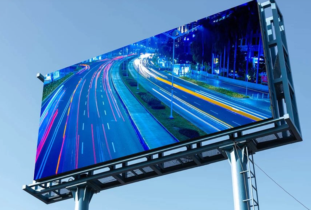
Display LED comuni (cartelloni pubblicitari interni/esterni, videowall), retroilluminazione per dispositivi elettronici di consumo (ad esempio, TV).
Tecnologia di confezionamento COB
Il COB (Chip on Board) integra direttamente più chip LED (rosso, verde, blu) sul substrato del PCB, seguito dall'incapsulamento con colla fluorescente e materiali protettivi, creando una superficie di emissione luminosa senza soluzione di continuità. Senza strutture a perline individuali, il COB prevede l'incollaggio diretto dei chip al substrato, con l'intero pannello ricoperto da materiali protettivi come il silicone.
Vantaggi:
- Elevata affidabilità; nessuna giuntura esposta, eccellente resistenza a polvere, umidità e urti, adatto ad ambienti difficili.
- Dissipazione del calore superiore poiché i chip sono a contatto diretto con il substrato, facilitando il rapido trasferimento del calore.
- Display uniforme con una superficie continua di emissione luminosa, che elimina gli spazi tra i pixel e garantisce un'esperienza visiva fluida, in particolare per display con passo ridotto.
- Lunga durata con bassi tassi di pixel morti e costi di manutenzione ridotti.
- Capacità di ottenere pixel pitch estremamente piccoli (ad esempio 0,9 mm, 0,7 mm, 0,43 mm).
Svantaggi:
- Difficili da riparare; in caso di guasti è spesso necessario sostituire l'intero modulo, con conseguente aumento dei costi.
- Investimento iniziale più elevato dovuto a processi complessi e infrastrutture industriali meno mature rispetto alla tecnologia SMD.
- Luminosità limitata poiché i materiali di incapsulamento possono influire sull'efficienza luminosa, richiedendo l'ottimizzazione per scenari ad alta luminosità.
Applicazioni tipiche:
Display per interni di alta gamma (sale conferenza, centri di comando), applicazioni industriali (mediche, monitoraggio della sicurezza) e tecnologie LED Mini/Micro all'avanguardia.
Guida alla selezione:
- Scegli SMD per progetti attenti al budget, che richiedono elevata luminosità o per situazioni di facile manutenzione (ad esempio, pubblicità esterna).
- Scegliete COB quando date priorità a elevata stabilità, affidabilità a lungo termine e display di piccole dimensioni (ad esempio, sale conferenze, centri di monitoraggio).
Sfide nello sviluppo dei display a LED: aberrazione cromatica nei display a passo piccolo
Aberrazione cromatica nei display con passo piccolo e ultra piccolo
Con l'aumento delle esigenze di qualità visiva, i display LED a passo piccolo (pixel pitch ≤2 mm) e ultra-piccolo (≤0,9 mm) stanno guadagnando popolarità per le loro immagini ad alta risoluzione. Tuttavia, devono affrontare un problema significativo: l'aberrazione cromatica.
Cause principali dell'aberrazione cromatica
- Incoerenza delle perle LED: Anche all'interno dello stesso lotto di produzione, le perle LED variano in luminosità e lunghezza d'onda del colore a causa di limitazioni di produzione. Nei display con passo ridotto, queste piccole differenze vengono amplificate, con conseguente incoerenza di colori e luminosità tra pixel adiacenti. Sia i COB che gli SMD sono interessati; il design integrato dei COB può concentrare l'impatto all'interno di un modulo, mentre le perle indipendenti degli SMD possono disperdere l'effetto sullo schermo.
- Limitazioni dei processi tradizionali delle maschere: I primi display a LED utilizzavano maschere nere sui PCB per bloccare gli spazi vuoti di luce e migliorare il contrasto. Per i display con passo piccolo e piccolissimo, la produzione tradizionale di maschere fatica a soddisfare i requisiti di precisione. Creare strutture sottili per passi pixel minuscoli e garantire un allineamento accurato con le perle è impegnativo, con conseguente scarsa schermatura della luce, maggiore dispersione della luce e differenze di colore accentuate. La natura integrata del COB rende le maschere tradizionali meno adattabili, mentre la tecnologia SMD, sebbene più regolabile, deve ancora affrontare problemi di precisione a passi piccoli.
- Dissipazione del calore ed effetti del circuito di azionamento: L'elevata densità di perle nei display a passo piccolo causa calore concentrato. Una dissipazione del calore inadeguata causa variazioni di colore poiché diverse aree del display si riscaldano in modo non uniforme. Anche le variazioni nei circuiti di pilotaggio possono causare correnti di pilotaggio incoerenti, influenzando la luminosità e il colore delle perle. Il COB, con chip collegati direttamente al PCB, ha un percorso di dissipazione del calore teorico più breve, ma richiede sofisticati progetti di dissipazione del calore del PCB. L'SMD, con perle collegate tramite staffe, ha un percorso di dissipazione del calore più complesso ed entrambi i metodi richiedono un'attenta ottimizzazione per mitigare l'aberrazione cromatica.

Maschera di sfondo manuale insertion
Tecnologia di iniezione della macchina erogatrice per attenuare l'aberrazione cromatica nei display a LED
Principio di funzionamento
Spruzzatura di precisione di inchiostri neri o colorati sul PCB dei display a LED o tra le unità pixel. Per i moduli COB, la stampa a getto d'inchiostro grafico tramite tecnologia di stampa crea maschere virtuali tra i pixel, riducendo significativamente la differenza di colore tra i moduli e migliorando il contrasto del display.
Soluzioni
1. Mascheratura dello sfondo
Funzione: copre il colore di base del PCB, che spesso causa tonalità di colore incoerenti sugli schermi di grandi dimensioni.
Implementazione: inchiostri speciali vengono spruzzati sul PCB mediante apparecchiature di distribuzione/getto d'inchiostro per garantire un colore uniforme dell'inchiostro, riducendo al minimo le deviazioni di colore causate dal colore di base del PCB che influisce sull'emissione LED.
2. Formazione della maschera integrata
Funzione: Crea una maschera integrata tra le unità pixel dei display LED, in particolare per i pacchetti COB.
Effetto: risolve gli spazi vuoti e le differenze di colore tra i moduli COB, previene la diafonia luminosa tra i pixel e garantisce una consistenza uniforme dei colori su tutto il display.
Note tecniche
Per ottimizzare il contrasto e l'uniformità del colore, vengono solitamente utilizzati inchiostri fotoindurenti con elevata capacità di assorbimento della luce (≥99,51 μm a 450-700 nm).
Raccomandazioni sull'attrezzatura

Clicca sul link per saperne di più sull'attrezzatura:Macchina di dosaggio di precisione ad alta velocità D450S: attrezzatura fondamentale per risolvere le differenze di colore nei display a LED
Erogazione di getto d'inchiostro nella produzione di LED
Nello sviluppo dei display a LED, le sfide principali includono pixel pitch ultra-stretti (ad esempio, P1.2/P0.9), rivestimento multistrato preciso, E adattamento complesso della superficie curva:
- Sfida del passo ultra-ristretto: La tecnologia di erogazione a getto d'inchiostro affronta la "distribuzione non uniforme della colla e i rischi di cortocircuito" tra chip LED ravvicinati attraverso controllo delle goccioline a livello di micron (gocce da 10-50 μm). Per gli imballaggi COB, la stampa a getto d'inchiostro precisa impedisce che la colla fuoriesca sugli elettrodi, migliorando l'uniformità dell'illuminazione.
- Rivestimento multistrato: Per le strutture OLED/mini LED (strati emissivi, strati dielettrici), la tecnologia a getto d'inchiostro consente impilamento multimateriale e multispessore (ad esempio, prima l'inchiostro emissivo, poi l'isolamento dielettrico), eliminando i problemi di "variazioni di spessore e miscelazione dei colori tra gli strati" dovuti al rivestimento tradizionale della lama, garantendo la purezza del colore.
- Adattamento della superficie curva: Per display flessibili/irregolari, la stampa a getto d'inchiostro senza contatto si adatta alle differenze di altezza della superficie, sostituendo la tradizionale erogazione ad aghi soggetta a "graffi e perdite", ampliando le possibilità di progettazione (ad esempio, schermi curvi per automobili, dispositivi indossabili).
L'uniformità degli strati di emissione luminosa influisce direttamente sulla coerenza della luminosità del display. La tecnologia di erogazione a getto d'inchiostro raggiunge risultati rivoluzionari tramite controllo preciso dell'inchiostro + processi intelligenti:
- Controllo della dispersione dell'inchiostro: Utilizzando valvole piezoelettriche per un'erogazione precisa dell'inchiostro (precisione di posizionamento ripetuto ±0,02 mm), garantisce un volume di goccioline e un posizionamento uniformi dei materiali emissivi (ad esempio, colla al fosforo, inchiostro a punti quantici), eliminando i "punti chiari/scuri" causati da una distribuzione non uniforme.
- Sinergia di essiccazione e stagionatura: Post-getto d'inchiostro, ricottura a temperatura controllata zonale (ad esempio, 80°C di pre-cottura + 120°C di polimerizzazione completa) risolve i problemi di "ritiro e spostamento dell'emissione luminosa" dovuti a un'essiccazione non uniforme, garantendo uniformità microstrutturale per una luminosità stabile.
- Coerenza da bordo a centro: Posizionamento guidato dalla vista regola dinamicamente i parametri del getto d'inchiostro (ad esempio, aumento del volume dell'inchiostro sui bordi per compensare la riflessione del substrato), garantendo uno spessore uniforme e una concentrazione del materiale su tutto lo schermo, eliminando gli effetti "centro luminoso, bordi scuri".
Le linee SMT puntano a un'automazione senza soluzione di continuità nelle fasi di "posizionamento-erogazione-saldatura-ispezione". La tecnologia di erogazione a getto d'inchiostro contribuisce attraverso:
- Sincronizzazione di precisione e tempistica: I sistemi a getto d'inchiostro si integrano con le macchine pick-and-place tramite Comunicazione PLC, avviando l'erogazione della colla lungo percorsi pre-programmati (ad esempio, rinforzo del pad PCB) con una precisione di ±20μm dopo il posizionamento del componente, riducendo al minimo il disallineamento indotto dall'errore umano.
- Interconnettività e tracciabilità dei dati: I parametri del getto d'inchiostro (volume, posizione, velocità) si integrano con i dati SMT (informazioni sui componenti, profili di saldatura), formando un catena dati completa. Per i lotti difettosi, le anomalie del volume del getto d'inchiostro consentono una rapida analisi della causa principale.
- Adattamento flessibile della produzione: Supporto per cambi rapidi di prodotto (software-driven program switching) collabora con i sistemi di alimentazione SMT per la transizione tra display di grande formato e display a passo stretto in meno di 10 minuti, ottimizzando la produzione di piccole quantità e di più varietà.